Abstract
Silicon spin qubits are promising candidates for realizing large-scale quantum processors, benefitting from a magnetically quiet host material and the prospects of leveraging the mature silicon device fabrication industry. We report the measurement of an electron spin in a singly occupied gate-defined quantum dot, fabricated using CMOS-compatible processes at the 300-mm wafer scale. For readout, we employ spin-dependent tunneling combined with a low-footprint single-lead quantum-dot charge sensor, measured using rf gate reflectometry. We demonstrate spin readout in two devices using this technique, obtaining valley splittings in the range 0.5–0.7 meV using excited-state spectroscopy, and measure a maximum electron-spin relaxation time () of s at 1 T. These long lifetimes indicate the silicon-nanowire geometry and fabrication processes employed here show a great deal of promise for qubit devices, while the spin-readout method demonstrated here is well suited to a variety of scalable architectures.
- Received 16 May 2020
- Revised 12 October 2020
- Accepted 24 February 2021
DOI:https://doi.org/10.1103/PRXQuantum.2.010353
Published by the American Physical Society under the terms of the Creative Commons Attribution 4.0 International license. Further distribution of this work must maintain attribution to the author(s) and the published article's title, journal citation, and DOI.
Published by the American Physical Society
Physics Subject Headings (PhySH)
Popular Summary
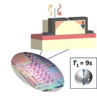
The same silicon technology used in conventional integrated circuits can be exploited for a physical realization of a qubit, the unit cell of a quantum computer. In this approach, information is encoded in the spin degree of freedom of an electron confined in a nanoscale semiconductor device known as a quantum dot. The small size of the quantum dots enables a high qubit density similar to the density of transistors in current processors. To reach the full potential in qubit density, and thus in quantum-computer performance, qubits need to be manufactured using industrial mass fabrication techniques while the footprint of circuits fabricated alongside each qubit for readout or control needs to be minimized. Our work addresses both issues, evaluating whether CMOS-compatible manufacturing processes performed at the scale of 300-mm wafers can be used to make long-lived spin qubits combined with a reduced-footprint readout method.
The readout of an electron spin trapped in the dot is performed by conditioning its tunneling to an electric reservoir on its spin polarization. Such a tunneling event disturbs the potential of a neighbor “sensor” dot, which is constantly monitored. To do so, a small oscillating rf signal sent to the sensor gate electrode is continuously attempting to move an electron between the sensor dot and the reservoir. The breakdown of this dynamic equilibrium due to spin-dependent tunneling is measured as a change in the dot capacitance.
Our results show long relaxation times measured using a compact readout setup, positioning CMOS-compatible devices as potential high-quality qubits compatible with scalable manufacturing.