Abstract
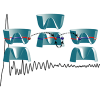
Electron optics in the solid state promises new functionality in electronics through the possibility of realizing nano- and micrometer-sized interferometers, lenses, collimators, and beam splitters that manipulate electrons instead of light. Until now, however, such functionality has been demonstrated exclusively in one-dimensional devices, such as in nanotubes, and in graphene-based devices operating with junctions. In this work, we describe a novel mechanism for realizing electron optics in two dimensions. By studying a two-dimensional Fabry-Perot interferometer based on a resonant cavity formed in an InAs/GaSb double quantum well using junctions, we establish that electron-hole hybridization in band-inverted systems can facilitate coherent interference. With this discovery, we expand the field of electron optics in two dimensions to encompass materials that exhibit band inversion and hybridization.
- Received 13 November 2019
- Revised 13 February 2020
- Accepted 29 April 2020
DOI:https://doi.org/10.1103/PhysRevX.10.031007
Published by the American Physical Society under the terms of the Creative Commons Attribution 4.0 International license. Further distribution of this work must maintain attribution to the author(s) and the published article’s title, journal citation, and DOI.
Published by the American Physical Society
Physics Subject Headings (PhySH)
Popular Summary
The main functional principle of optical interferometers is the interference of monochromatic waves that propagate in the same direction. In such interferometers, the interference can be observed as a periodic oscillation of the transmitted intensity upon varying the wavelength of the light. However, the period of the interference pattern strongly depends on the incident angle of the light, and as a result, the interference pattern is averaged out if light of all possible incident angles is sent through the interferometer at once. The same arguments apply to the interference of matter waves as described by quantum mechanics and, in particular, to electronic interferometers in which electrons interfere. Here, we investigate the phenomenon of electronic interference in a solid-state system consisting of two coupled semiconductor layers, InAs and GaSb.
We discover that these systems provide a novel transport mechanism that guarantees nonvanishing interference even under all angles of incidence. The mechanism arises from two properties of the InAs/GaSb system: band inversion, in which the usual ordering of conduction and valence bands is swapped, and hybridization, where the aforementioned bands mix, forming hybrid states. Using a combination of transport measurements and theoretical modeling, we describe the resulting operation of a Fabry-Perot interferometer in which electrons and holes form hybrid states and interfere.
Our results transcend InAs/GaSb systems, as the reported mechanism requires solely the two aforementioned ingredients of band inversion and hybridization. We therefore set the stage for engineering electron optics phenomena in a variety of materials, such as thin mono- and dichalcogenides as well as other 2D and 3D topological insulators.


